ī¦ļŖ▒Ī─ż╗∙ĄūCVD╩»─½Ž®,PET╗∙å╬īė╩»─½Ž®,PET╗∙å╬▒┌╠╝╝{├ū╣▄,╩»ėó╗∙å╬īė╩»─½Ž®,▓Ż┴¦╗∙å╬īė╩»─½Ž® |
 |
CVD╩»─½Ž®Ż║ī¦ļŖ▒Ī─ż╗∙Ąū
CVD Graphene on Conductive Coatings
Monolayer Graphene on PET,
PET╗∙å╬īė╩»─½Ž®
Single Walled Carbon Nanotubes on PET,
PET╗∙å╬▒┌╠╝╝{├ū╣▄
Monolayer Graphene film on Quartz, ╩»ėó╗∙å╬īė╩»─½Ž®
Monolayer Graphene on Glass,
▓Ż┴¦╗∙å╬īė╩»─½Ž®
CVD╩»─½Ž®Ż║ī¦ļŖ▒Ī─ż╗∙Ąū CVD Graphene on Conductive Coatings |
|||
| Monolayer Graphene on PET PET╗∙å╬īė╩»─½Ž® |
1Ī▒ Ī┴1Ī▒ |  |
Monolayer graphene film is grown by CVD processing onto copper foil, then transferred onto PET (Polyethylene terephthalate) Properties of Graphene Film on PET: The graphene coverage is about 95% The graphene film is continuous, with occasional holes and cracks The graphene film is polycrystalline, i.e. it consists of grains with different crystallographic orientation Sheet resistance 660-1500 ”Ė/Ī§ PET Thickness: 7 mil=175 micron Please note that it is difficult to obtain a Raman spectrum of graphene film directly on PET due to a strong background signal. We can manufacture custom, large-size coatings, and use different shapes and types of plastic materials. You may also send us your own substrates for coating. Few-layer graphene coatings with a lower sheet resistance and lower transparency can also be prepared. Please contact us for a quote. Our graphene films are made by a PMMA assisted transfer method. |
| 1Ī▒ Ī┴1Ī▒ 5Ų¼ | |
||
| 2Ī▒ Ī┴2Ī▒ | 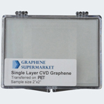 |
||
| Single Walled Carbon Nanotubes on PET PET╗∙å╬▒┌╠╝╝{├ū╣▄ |
1Ī▒ Ī┴1Ī▒ |  |
Single-Walled Carbon Nanotube Coatings Specifications: Transparency: 83%~90% at 550 nm wavelength Sheet Resistance: 600~1800 ”Ė/Ī§ PET Thickness: 7 mil=175 micron ═Ė▀^┬╩Ū·ŠĆ / Ąõą═SEMłDŽ±1 / Ąõą═SEMłDŽ±2 |
| 1Ī▒ Ī┴1Ī▒ 5Ų¼ | |
||
| Monolayer Graphene film on Quartz ╩»ėó╗∙å╬īė╩»─½Ž® |
1Ī▒ Ī┴1Ī▒ |  |
Monolayer graphene film is grown by CVD processing onto copper foil, then transferred onto quartz Properties of Graphene Film on Quartz: The thickness and quality of graphene films is controlled by Raman Spectroscopy The graphene coverage of this product is about 95% The graphene film is continuous, with occasional holes and cracks The graphene film is polycrystalline, i.e. it consists of grains with different crystallographic orientation The transmission of our graphene film is above 97% Sheet Resistance: 660-1,500 ”Ė/Ī§ Properties of Quartz Substrate: We use G.E. 124 Fused Quartz Substrates Knoop Hardness: >600 Kg/mm2 Density: 2.21 g/cm3 └Ł┬³╣ŌūVłD |
| 1Ī▒ Ī┴1Ī▒ 5Ų¼ | 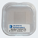 |
||
| Monolayer Graphene on Glass ▓Ż┴¦╗∙å╬īė╩»─½Ž® |
1Ī▒ Ī┴1Ī▒ 5Ų¼ |  |
Monolayer graphene film is grown by CVD processing onto copper foil, then transferred onto glass Properties of Graphene Film on Glass: The thickness and quality of graphene films is controlled by Raman Spectroscopy The graphene coverage of this product is about 95% The graphene film is continuous, with occasional holes and cracks The graphene film is polycrystalline, i.e. it consists of grains with different crystallographic orientation The transmission of our graphene film is above 97% Sheet Resistance: 660-1,500 ”Ė/Ī§ Properties of Glass Substrate: We use Corning EAGLE XGTM AMLCD Glass Substrates Thickness: 0.7 mm Density: 2.38 g/cc └Ł┬³╣ŌūVłD |
| 2Ī▒ Ī┴2Ī▒ | 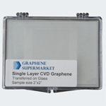 |
||
|
╔Ž║Ż▓Ż╔½ųŪ─▄┐Ų╝╝ėąŽ▐╣½╦Š ╔Ž║Ż: (021)3353-0926, 3353-0928 ▒▒Š®: (010)8217-0506 ÅVų▌: 139-0221-4841 ╬õØh: 139-1733-4172 ╚½ć°õN╩█Ę■䚤ߊƯ║4006-171751 Email: info@bosontech.com.cn www.gzrqr.com 2008-2022 All Rights Reserved! |
|
¤ßķT«aŲĘŻ║╣Ō└w╣ŌūVāxĪóĘeĘųŪ“ĪóŠ∙ä“╣Ōį┤ĪóSEMROCK×V╣ŌŲ¼Īó╠½║šŲØŽĄĮyĪó×V╣ŌŲ¼Īó╩»─½Ž®╝{├ū▓─┴Ž £¹ICPéõ09026157╠¢-2 |
|