SiO2/Si╗∙ĄūCVD╩»─½Ž®,╩»─½Ž®╠ūčbŻ¼SiO2╗∙Ąūå╬īė╩»─½Ž®Ż¼SiO2╗∙Ąūå╬/ļpīė╩»─½Ž® |
 |
CVD╩»─½Ž®Ż║SiO2/Si╗∙Ąū
CVD Graphene on SiO2/Si
Graphene Film Trial Kit, ╩»─½Ž®╠ūčb
Monolayer Graphene on 285 nm SiO2 Wafer,
285nm SiO2╗∙Ąūå╬īė╩»─½Ž®
Monolayer Graphene on 90 nm SiO2 Wafer,
90nm SiO2╗∙Ąūå╬īė╩»─½Ž®"
Single/Double Layer Graphene on 285 nm Silicon Dioxide Wafer, 285nm SiO2╗∙Ąūå╬/ļpīė╩»─½Ž®
Single/Double Layer Graphene on 90 nm Silicon Dioxide Wafer,
90nm SiO2╗∙Ąūå╬/ļpīė╩»─½Ž®
CVD╩»─½Ž®Ż║SiO2/Si╗∙Ąū CVD Graphene on SiO2/Si |
|||
| Graphene Film Trial Kit ╩»─½Ž®─ż╠ūčb |
ĪĪ | 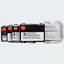 |
Includes: Two Single/Double Layer Graphene samples on 285 nm Silicon Dioxide Wafers: 1cm x 1 cm Two 10mmx10mm samples, Graphene Film on Nickel: 1 cm x 1 cm One sample of Multilayer Graphene on a 285 nm Silicon Dioxide Wafer: 1 cm x 1 cm One sample of Monolayer Graphene on a 285 nm Silicon Dioxide Wafer: 1 cm x 1 cm One sample of Monolayer Graphene on Glass: 1" x 1" If you are interested in investigating numerous different samples of graphene coatings, this trial kit is ideal. All of the samples are made by Chemical Vapor Deposition and give a strong Raman signal. A great value for students and scientific researchers alike interested in trying different samples. |
| Monolayer Graphene on 285 nm SiO2 Wafer 285nm SiO2╗∙Ąūå╬īė╩»─½Ž® |
4Ī▒ (100mm) wafer | 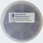 |
Monolayer graphene on silicon wafers (p-doped) with a 285 nanometer silicon dioxide coating. Properties of Graphene Film: The thickness and quality of our graphene films is controlled by Raman Spectroscopy The graphene coverage of this product is about 95% The graphene film is continuous, with occasional holes and cracks The graphene film is polycrystalline, i.e. it consists of grains with different crystallographic orientation Sheet Resistance: 660-1,500 ”Ė/Ī§ Our graphene films are predominantly single-layer graphene (more than 97%) with occasional small multilayer islands. Properties of Silicon/Silicon Dioxide Wafers: Oxide Thickness: 285 nm Color: Violet Wafer thickness: 525 micron Resistivity: 0.001-0.005 ohm-cm Type/Dopant: P/Boron Orientation: <100> Front Surface: Polished Back Surface: Etched Our graphene films are manufactured using a PMMA assisted transfer method. └Ł┬³╣ŌūVłD / ╣ŌīW(xu©”)łDŽ± / 4Ī▒ (100mm) wafer │▀┤ńłD |
| 10mmĪ┴10mm 10Ų¼ | 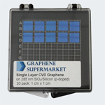 |
||
| 10mmĪ┴10mm 5Ų¼ |  |
||
| Monolayer Graphene on 90 nm SiO2 Wafer 90nm SiO2╗∙Ąūå╬īė╩»─½Ž® |
10mmĪ┴10mm 5Ų¼ | 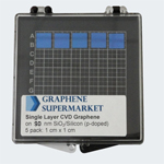 |
Monolayer graphene on silicon wafers with 90 nanometer silicon dioxide coating. Properties of Graphene Film: The thickness and quality of our graphene films is controlled by Raman Spectroscopy The graphene coverage of this product is about 95% The graphene film is continuous, with occasional holes and cracks The graphene film is polycrystalline, i.e. it consists of grains with different crystallographic orientation Sheet Resistance: 660-1,500 ”Ė/Ī§ Our graphene films are predominantly single-layer graphene (more than 97%) with occasional small multilayer islands. Properties of Silicon/Silicon Dioxide Wafers: Oxide Thickness: 90 nm Color: Violet Wafer thickness: 525 micron Resistivity: 0.001-0.005 ohm-cm Type/Dopant: P/Boron Orientation: <100> Front Surface: Polished Back Surface: Etched Our graphene films are manufactured using a PMMA assisted transfer method. └Ł┬³╣ŌūVłD / ╣ŌīW(xu©”)łDŽ± |
| Single/Double Layer Graphene on 285 nm Silicon Dioxide Wafer 285nm SiO2╗∙Ąūå╬/ļpīė╩»─½Ž® |
10mmĪ┴10mm 10Ų¼ | |
Mono and bilayer graphene on silicon wafers (p-doped) with a 285 nanometer silicon dioxide coating. The samples have nearly full monolayer coverage with 10-30% coverage of bilayer graphene islands. They are a great low-cost alternative to monolayer graphene for select purposes. Properties of Graphene Film: The graphene coverage of this product is about 95% The graphene film is continuous, with occasional holes and cracks The graphene film is polycrystalline, i.e. it consists of grains with different crystallographic orientation Properties of Silicon/Silicon Dioxide Wafers: Oxide Thickness: 285 nm Color: Violet Wafer thickness: 525 micron Resistivity: 0.001-0.005 ohm-cm Type/Dopant: P/Boron Orientation: <100> Front Surface: Polished Back Surface: Etched Our graphene films are manufactured using a PMMA assisted transfer method. ╣ŌīW(xu©”)łDŽ± / Ąõą═SEMłDŽ± |
| Single/Double Layer Graphene on 90 nm Silicon Dioxide Wafer 90nm SiO2╗∙Ąūå╬/ļpīė╩»─½Ž® |
10mmĪ┴10mm 10Ų¼ | |
Mono and bilayer graphene on silicon wafers (p-doped) with a 90 nanometer silicon dioxide coating. The samples have nearly full monolayer coverage with 10-30% coverage of bilayer graphene islands. They are a great low-cost alternative to monolayer graphene for select purposes. Properties of Graphene Film: The graphene coverage of this product is about 95% The graphene film is continuous, with occasional holes and cracks The graphene film is polycrystalline, i.e. it consists of grains with different crystallographic orientation Properties of Silicon/Silicon Dioxide Wafers: Oxide Thickness: 90 nm Color: Violet Wafer thickness: 525 micron Resistivity: 0.001-0.005 ohm-cm Type/Dopant: P/Boron Orientation: <100> Front Surface: Polished Back Surface: Etched Our graphene films are manufactured using a PMMA assisted transfer method. ╣ŌīW(xu©”)łDŽ± / Ąõą═SEMłDŽ± |
|
╔Ž║Ż▓Ż╔½ųŪ─▄┐Ų╝╝ėąŽ▐╣½╦Š ╔Ž║Ż: (021)3353-0926, 3353-0928 ▒▒Š®: (010)8217-0506 ÅVų▌: 139-0221-4841 ╬õØh: 139-1733-4172 ╚½ć°(gu©«)õN╩█Ę■äš(w©┤)¤ßŠĆŻ║4006-171751 Email: info@bosontech.com.cn www.gzrqr.com 2008-2022 All Rights Reserved! |
|
¤ßķT«a(ch©Żn)ŲĘŻ║╣Ō└w╣ŌūVāxĪóĘeĘųŪ“ĪóŠ∙ä“╣Ōį┤ĪóSEMROCK×V╣ŌŲ¼Īó╠½║šŲØŽĄĮy(t©»ng)Īó×V╣ŌŲ¼Īó╩»─½Ž®╝{├ū▓─┴Ž £¹ICPéõ09026157╠¢(h©żo)-2 |
|